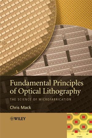
Fundamental Principles of Optical Lithography: The Science of MicrofabricationISBN: 978-0-470-01893-4
Hardcover
534 pages
January 2008
 This is a Print-on-Demand title. It will be printed specifically to fill your order. Please allow an additional 10-15 days delivery time. The book is not returnable.
Other Available Formats: Paperback
|
||||||
1. Introduction to Semiconductor Lithography.
1.1 Basics of IC Fabrication.
1.2 Moore’s Law and the Semiconductor Industry.
1.3 Lithography Processing.
Problems.
2. Aerial Image Formation – The Basics.
2.1 Mathematical Description of Light.
2.2 Basic Imaging Theory.
2.3 Partial Coherence.
2.4 Some Imaging Examples.
Problems.
3. Aerial Image Formation – The Details.
3.1 Aberrations.
3.2 Pupil Filters and Lens Apodization.
3.3 Flare.
3.4 Defocus.
3.5 Imaging with Scanners Versus Steppers.
3.6 Vector Nature of Light.
3.7 Immersion Lithography.
3.8 Image Quality.
Problems.
4. Imaging in Resist: Standing Waves and Swing Curves.
4.1 Standing Waves.
4.2 Swing Curves.
4.3 Bottom Antirefl ection Coatings.
4.4 Top Antirefl ection Coatings.
4.5 Contrast Enhancement Layer.
4.6 Impact of the Phase of the Substrate Refl ectance.
4.7 Imaging in Resist.
4.8 Defi ning Intensity.
Problems.
5. Conventional Resists: Exposure and Bake Chemistry.
5.1 Exposure.
5.2 Post-Apply Bake.
5.3 Post-exposure Bake Diffusion.
5.4 Detailed Bake Temperature Behavior.
5.5 Measuring the ABC Parameters.
Problems.
6. Chemically Amplifi ed Resists: Exposure and Bake Chemistry.
6.1 Exposure Reaction.
6.2 Chemical Amplifi cation.
6.3 Measuring Chemically Amplifi ed Resist Parameters.
6.4 Stochastic Modeling of Resist Chemistry.
Problems.
7. Photoresist Development.
7.1 Kinetics of Development.
7.2 The Development Contrast.
7.3 The Development Path.
7.4 Measuring Development Rates.
Problems.
8. Lithographic Control in Semiconductor Manufacturing.
8.1 Defi ning Lithographic Quality.
8.2 Critical Dimension Control.
8.3 How to Characterize Critical Dimension Variations.
8.4 Overlay Control.
8.5 The Process Window.
8.6 H–V Bias.
8.7 Mask Error Enhancement Factor (MEEF).
8.8 Line-End Shortening.
8.9 Critical Shape and Edge Placement Errors.
8.10 Pattern Collapse.
Problems.
9. Gradient-Based Lithographic Optimization: Using the Normalized Image Log-Slope.
9.1 Lithography as Information Transfer.
9.2 Aerial Image.
9.3 Image in Resist.
9.4 Exposure.
9.5 Post-exposure Bake.
9.6 Develop.
9.7 Resist Profi le Formation.
9.8 Line Edge Roughness.
9.9 Summary.
Problems.
10. Resolution Enhancement Technologies.
10.1 Resolution.
10.2 Optical Proximity Correction (OPC).
10.3 Off-Axis Illumination (OAI).
10.4 Phase-Shifting Masks (PSM).
10.5 Natural Resolutions.
Problems.
Appendix A. Glossary of Microlithographic Terms.
Appendix B. Curl, Divergence, Gradient, Laplacian.
Appendix C. The Dirac Delta Function.
Index.


