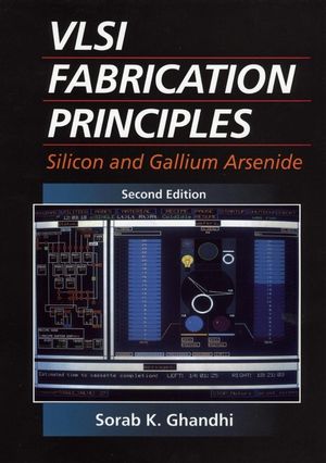
VLSI Fabrication Principles: Silicon and Gallium Arsenide, 2nd EditionISBN: 978-0-471-58005-8
Hardcover
864 pages
March 1994
 This is a Print-on-Demand title. It will be printed specifically to fill your order. Please allow an additional 15-20 days delivery time. The book is not returnable.
|
||||||
1 Material Properties 1
1.1 Physical Properties 3
1.2 Crystal Structure 13
1.3 Crystal Axes and Planes 16
1.4 Orientation Effects 19
1.5 Point Defects 23
1.6 Dislocations 45
1.7 Electronic Properties of Defects 53
Tables 58
References 64
Problems 67
2 Phase Diagrams and Solid Solubility 69
2.1 Unitary Diagrams 70
2.2 Binary Diagrams 70
2.3 Solid Solubility 88
2.4 Ternary Diagram 91
References 99
Problem 100
3 Crystal Growth and Doping 102
3.1 Starting Growth and Doping 102
3.2 Growth from the Melt 106
3.3 Considerations for Proper Crystal Growth 113
3.4 Doping in the Melt 120
3.5 Semi-Insulating Gallium Arsenide 129
3.6 Properties of Melt-Grown Crystals 132
3.7 Solution Growth 134
3.8 Zone Processes 135
3.9 Properties of Zone-Processed Crystals 141
Tables 142
References 145
Problems 149
4 Diffusion 150
4.1 The Nature of Diffusion 151
4.2 Diffusion in a Concentration Gradient 154
4.3 The Diffusion Equation 171
4.4 Impurity Behavior: Silicon 183
4.5 Impurity Behavior: Gallium Arsenide 197
4.6 Diffusion Systems 202
4.7 Diffusion Systems for Silicon 209
4.8 Special Problems in Silicon Diffusion 217
4.9 Diffusion Systems for Gallium Arsenide 224
4.10 Evaluation Techniques for Diffused Layers 235
Tables 246
References 251
Problems 256
5 Epitaxy 258
5.1 General Considerations 261
5.2 Molecular Beam Epitaxy 273
5.3 Vapor-Phase Epitaxy 283
5.4 VPE Processes for Silicon 296
5.5 VPE Processes for Gallium Arsenide 313
5.6 Liquid-Phase Epitaxy 330
5.7 LPE Systems 340
5.8 Heteroepitaxy 345
5.9 Evaluation of Epitaxial Layers 348
Tables 356
References 358
Problems 366
6 Ion Implantation 368
6.1 Penetration Range 370
6.2 Implantation Damage 389
6.3 Annealing 393
6.4 Ion Implantation Systems 407
6.5 Process Considerations 416
6.6 High-Energy Implants 430
6.7 High-Current Implants 431
6.8 Application to Silicon 432
6.9 Application to Gallium Arsenide 437
Tables 442
References 443
Problems 449
7 Native Films 451
7.1 Thermal Oxidation of Silicon 452
7.2 Thermal Nitridation of Silicon 483
7.3 Thermal Oxidation of Gallium Arsenide 485
7.4 Anodic Oxidation 487
7.5 Plasma Processes 495
7.6 Evaluation of Native Films 498
Tables 500
References 503
Problems 508
8 Deposited Films 510
8.1 Film Deposition Methods 511
8.2 Film Characteristics 522
8.3 Films for Protection and Masking 527
8.4 Films for Doping 546
8.5 Films for Interconnections 548
8.6 Films for Ohmic Contacts 556
8.7 Films for Schottky Diodes 570
Tables 576
References 578
9 Etching and Cleaning 587
9.1 Wet Chemical Etching 589
9.2 Dry Physical Etching 613
9.3 Dry Chemical Etching 620
9.4 Reactive Ion Etching 625
9.5 Chemically Assisted Ion Beam Techniques 636
9.6 Etching-Induced Damage 638
9.7 Cleaning 639
Tables 646
References 654
Problems 661
10 Lithographic Processes 662
10.1 Photoreactive Materials 664
10.2 Pattern Generation and Mask-Making 669
10.3 Pattern Transfer 674
10.4 Advanced Techniques 685
10.5 Problem Areas 696
11 Device and Circuit Fabrication 704
11.1 Isolation 705
11.2 Self-Alignment 712
11.3 Local Oxidation 714
11.4 Planarization 721
11.5 Metallization 726
11.6 Gettering 728
11.7 Mos-Based Silicon Microcircuits 730
11.8 BJT-Based Silicon Microcircuits 749
11.9 Gallium Arsenide Microcircuits 778
Tables 790
References 790
Appendix The Mathematics of Diffusion 801
A.1 Solutions for a Constant Diffusion Coefficient 802
A.2 Solution for a Time-Dependent Diffusion Coefficient 811
A.3 Solution for Concentration-Dependent Diffusion Coefficients 813
A.4 Determination of the Diffusion Constant 815
References 817
Index 819


